Introduction to HBM
What is HBM?
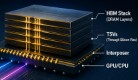
HBM (High Bandwidth Memory) is a type of stacked DRAM designed specifically for AI computing and high-performance processors. It vertically stacks multiple chips using through-silicon via (TSV) technology, increasing bandwidth and energy efficiency by more than ten times compared to traditional memory, making it a key foundation for AI chips to process massive amounts of data.
HBM vs. Traditional Memory
HBM essentially involves vertically stacking multiple layers of DRAM and connecting them to AI accelerators via TSV (Through Silicon Vias) and ultra-wide interfaces. Traditional memory primarily increases frequency, while HBM expands a narrow road into a multi-lane highway by adding parallel channels.
Traditional memory (such as DDR and GDDR) is like a single-lane highway; although capacity can be increased by increasing speed (frequency), there are physical limits to speed. With the explosion of large-scale AI models (LLM), computing chips (GPUs).
The Importance of HBM
Why has HBM become a bottleneck for AI?
GPU performance improvements increasingly rely on simultaneous upgrades to memory capacity and bandwidth.
During token-by-token inference, the system needs to repeatedly read model weights and update and access the key-value cache. The larger the model, the longer the context, and the more concurrent users, the more data needs to be moved.
While computing units can quickly complete matrix operations, they may wait for the next batch of data to arrive for a long time.
The concept of “AI as memory” doesn’t mean computing chips have lost their value, but rather that the system bottleneck has shifted from simple floating-point computing power to a balance between computing power, bandwidth, capacity, and interconnectivity.
Simply increasing GPU area without improving memory supply capacity makes it difficult to fully utilize the increased computing power. Therefore, HBM is gradually becoming a core strategic asset for AI.
Memory vendors bargaining power is rising
The training phase requires extremely high computing power, but tasks are typically concentrated in a few large clusters; the inference phase, however, deals with massive users, long contexts, multimodal inputs, and continuously running AI agents.
As AI moves from model development to commercial deployment, the demands on memory capacity, bandwidth, and power consumption for inference may become more persistent.
This shift is driving HBM from standardized products to customized system components. HBM4 introduces more complex logic substrate chips, allowing memory control, interfaces, and some computing functions to be co-designed based on the accelerator architectures of customers such as NVIDIA, Google, Microsoft, and AMD.
Memory manufacturers are no longer just producing general-purpose chips; they are involved in system definition from the early stages of R&D. Customization means longer certification cycles, higher switchover costs, and earlier capacity lock-in.
Customers need to determine specifications and delivery times in advance, while suppliers arrange wafer, packaging, and equipment investments according to long-term agreements. Standardized procurement is shifting towards a shared responsibility for R&D and capacity risks.
However, the notion of a complete reversal between the two parties is still an oversimplification. NVIDIA and cloud providers, controlling system architecture, software ecosystems, and final orders, still possess significant bargaining power.
Samsung, SK Hynix, and Micron, on the other hand, have gained greater influence through technology, yield rates, and limited production capacity. The real change is that memory has transformed from a replaceable component into a critical element influencing the time-to-market of the entire platform.
For SK Hynix, please see my post of “SK Hynix dominates memory by AI“.
The born of HBM
The Original Idea for HBM Came from AMD
This idea was not original to SK Hynix. The idea of 3D stacked DRAM was proposed as early as the 1990s, but it remained unrealized due to yield and cost constraints. It was AMD (ticker: AMD) that truly brought HBM from research paper to product.
In 2013, AMD was searching for memory solutions for its next-generation GPUs. They discovered that traditional GDDR5 bandwidth had reached its limit; even with a frequency of 7Gbps and a 512-bit bus width, it could only provide less than 360GB/s of bandwidth, far from sufficient to meet the terrifying parallel computing demands of future GPUs. AMD proposed a bold idea: to integrate the memory and GPU core onto the same silicon interposer, using a wider interface (1024-bit) and lower voltage to achieve a several-fold increase in bandwidth.
This was the prototype of HBM. During the early stages of HBM research and implementation at AMD, SK Hynix was AMD’s closest and most active partner.
SK Hynix was the first developer of HBM
In 2013, SK Hynix applied TSV (Through Silicon Via) technology to DRAM, successfully developing the first generation of high-bandwidth memory, HBM.
In early 2014, SK Hynix fabricated its first 4-Hi (4-layer stacked) HBM sample at its Icheon plant in Gyeonggi Province, South Korea. It was a silicon wafer the size of a fingernail, only about 200 micrometers thick, with four 2Gb DRAM dies vertically interconnected through approximately 5000 TSV channels.
AMD secured the first commercial order. In June 2015, the AMD Radeon R9 Fury X was released, the world’s first commercially available product featuring HBM. Its 512GB/s bandwidth was approximately 1.5 times that of the contemporary GTX 980 Ti.
HBM1 debut failed to win PO
HBM1 gained reputation in the market, but not in the form of orders.
Fury X sales fell short of expectations, and AMD’s GPU business subsequently slumped for several years. From 2016 to 2019, the HBM1 and HBM2 markets were virtually frozen by the slow-burning growth of AI and high-end graphics cards.
During that period, SK Hynix’s HBM team held a delicate position within the company. Financially, the HBM business consistently showed losses or broke even; before the AI boom, HBM was merely a hidden gem.
But SK Hynix didn’t stop. In January 2016, JEDEC officially released the HBM2 standard, with SK Hynix as a core member; in 2018, they were the first in the industry to mass-produce 8-Hi HBM2.
HBM is the key of AI computing
AI brought renewed attention to HBM
Until AI arrived. In 2020, OpenAI launched GPT-3, triggering a surge in global demand for AI computing power. However, from 2020 to the first half of 2022, SK Hynix did not truly reap the benefits of AI. The company was still struggling at the tail end of the storage downturn cycle.
The core of AI computation is memory, not GPU.
“Even if you install 1 million NVIDIA GPUs, they only utilize about 10% of the memory,” said Kim Jung-ho, a professor at the Korea Advanced Institute of Science and Technology (KAIST) known as the father of HBM, in a recent interview. The remaining 90% of the time, the GPU waits for data to arrive from memory, essentially remaining idle. Kim Jung-ho, the father of HBM: AI is essentially memory.
The reason is simple. Every time AI outputs a word, it needs to read data from the HBM and rewrite it, and this read/write time consumes almost all of the time.
Even with optimized algorithms, GPUs rarely exceed 30% utilization. Therefore, Professor Kim emphasizes that AI capabilities are ultimately determined by memory; AI is essentially memory.
The signs of this shift are also clear. With the transition from the training era to the inference era, the demand for memory has exploded. Starting with HBM4, it is no longer a standard product but rather a customized production based on pre-agreed quantities with customers.
The duopoly of Samsung and SK Hynix
This is a market where buyers no longer dominate and sellers determine prices; the roles of buyer and seller are completely reversed. This is why the projected combined operating profit of Samsung Electronics and SK Hynix reaching 500-600 trillion won is not unfounded.
The Next Step for HBM
HBF and HBS form a hierarchical memory
HBM solved the speed problem but is still limited by capacity, cost, and package area. As model parameters, key-value cache, and multimodal data continue to grow, storing all data in expensive DRAM in the long term is uneconomical. HBF thus becomes the next technological route.
HBF can be understood as stacking NAND Flash in a highly parallel manner, providing greater capacity in a physical form close to HBM.
Sandisk (ticker:SNDK) has proposed achieving approximately 8 to 16 times the capacity of HBM at a similar cost and plans to provide the first samples in the second half of 2026 and begin sampling inference devices equipped with HBF in early 2027.
HBF is slower than HBM but has greater capacity and lower unit cost, making it suitable for storing read-intensive data such as model weights.
In the future, a hierarchical structure may emerge: HBM handles “hot data,” HBF stores “cold data,” and ordinary SSDs and network memory reside in a lower layer. Data moves between different layers based on access frequency. HBF is not a replacement for HBM, but rather adds a new capacity layer for the inference era.
Kim Jung-ho, a professor at the Korea Advanced Institute of Science and Technology (KAIST) known as the father of HBM, further proposed HBS, or High Bandwidth SRAM. SRAM has lower latency, but is expensive and has low density, traditionally only used as on-chip cache.
If wafer-level, multi-layer stacking can be achieved in the future, HBS could become the ultra-high-speed memory closest to the computing unit. However, HBS is currently still a cutting-edge concept, far from standardization and commercial mass production; yield, power consumption, and heat dissipation are real obstacles.
Future winners won’t just be GPU companies
A traditional AI server, broken down, resembles a flat “technology park”: the GPU is located in the city center, HBM memory is like several tall buildings surrounding it, while NAND flash memory and SRAM are scattered further out. Data travels between these layers, still traversing long, energy-intensive “surface highways.”
As HBM, HBF, and HBS mature, future AI chips may no longer be simply “a few memory chips next to a GPU,” but rather a 3D system composed of logic chips, DRAM, NAND, and SRAM.
The GPU or CPU handles computation, HBM provides high-speed bandwidth, HBF provides large capacity, HBS acts as an ultra-low latency cache, and power and cooling are integrated throughout the entire package.
This will redistribute value in the semiconductor industry. NVIDIA’s computing architecture and CUDA ecosystem still constitute a strong barrier, and GPU performance has not stopped growing, but system performance increasingly depends on memory, advanced packaging, interconnects, power supply, and heat dissipation. The value of AI servers will expand from the GPU die to HBM, logic substrate, silicon interposer, liquid cooling, and power systems.
Samsung and SK Hynix have the advantage of possessing DRAM, NAND, HBM, and advanced packaging capabilities simultaneously, but this combination is not unique to Korean companies; Micron also covers DRAM, NAND, and HBM.
Korea’s true leadership lies in its HBM mass production experience, customer certification, and manufacturing ecosystem. Meanwhile, Chinese companies like Changxin Memory are also advancing the R&D of high-end DRAM and HBM. Technological gaps, yield rates, and customer validation will continue to determine the speed of catch-up.
The market’s projection of Samsung and SK Hynix’s combined future operating profit to trillions of won is clearly an overly aggressive scenario based on a supercycle, rather than company guidance or consensus expectations.
Customized HBMs do improve order visibility and profit margins, but capacity expansion, customer concentration, geopolitics, and technological iterations can still alter the outcome.
The traditional computing power arms race has reached a dead end. The next round of competition in AI architecture appears to be about who can do better power supply and heat dissipation, but the underlying logic remains that all of this serves to “get data to memory faster and more energy-efficiently.”
Whoever can break down the “memory wall” first will truly unleash the full potential of large-scale models. Currently, it seems that the next generation of AI computing architecture will ultimately be defined by DRAM memory.
Related articles
- “How was HBM born? Why HBM is important to AI?“
- “SK Hynix dominates memory by AI“
- “Sandisk soared 50-fold in 1.5 years, driven by AI demand“
- “Western Digital saw 200% annual stock performance,thanks to AI“
- “Seagate comeback thanks to AI, No 1 S&P 500 perform stocks YTD“
- “AI inference chips vs. training chips“
- “How GPU farms CoreWeave make money?“
- “Geoffrey Hinton, 2024 Nobel Physics winner, inadvertently helped Nvida transform to AI overlord“
- “Top vendors and uses of GPU“
- “How does CUDA strengthen the moat of Nvidia’s monopoly?“
- “Comparison of AI chips GPU and ASIC“
- “ASIC market is getting bigger, and related listed companies in the US and Taiwan“
- “How AMD makes money? A rare case of turning defeat into victory“
- “Why is AMD’s performance so jaw-dropping?“
- “Significant changes in Broadcom’s business approach“
- “The reasons behind Broadcom share price consistantly outperformance“
- “How low-key Marvell makes money?“
- “How does nVidia make money, Nvidia is changing the gaming rules“
- “The reasons for Nvidia’s monopoly and the challenges it faces“
- “Why nVidia failed to acquire ARM?“
- “Revisiting Nvidia: The Absolute Leader in Artificial Intelligence, Data Center, and Graphics“
- “Data center, a rapidly growing semiconductor field“
Disclaimer
- The content of this site is the author’s personal opinions and is for reference only. I am not responsible for the correctness, opinions, and immediacy of the content and information of the article. Readers must make their own judgments.
- I shall not be liable for any damages or other legal liabilities for the direct or indirect losses caused by the readers’ direct or indirect reliance on and reference to the information on this site, or all the responsibilities arising therefrom, as a result of any investment behavior.