Foreword
The reason to have this post
This post will discuss the semiconductor industry and the cost, sell price, and R&D cost of chip foundry that most Taiwan stock investors are concerned about, including the client and the main costs of wafer foundry manufacturers.
Source
My main sources of information are:
- Public information published by these five companies.
- Information published by media around the world.
Update frequency
Since there are more than tens of thousands of people readers following this article from around the world, I will update this post as often as possible.
Companion posts to this article
Readers who will read this article, I guess you will be very interested in the sister post of this post you are reading now. You are welcome to click “Comparison of SMIC, Rapidus, TSMC, Intel, and Samsung’s new process roadmaps for future chips“, “Yield rate comparison of SMIC, Rapidus, TSMC, Samsung, Intel’s advanced process“, “How many fabs and houses does TSMC have currently and in the future?” and”The TSMC cost, sell price, and R&D cost of chip foundry“
TSMC discussion in my books
I have discussed the company Nvidia (ticker:NVDA) in two recent books; including:
In my book “The Rules of Super Growth Stocks Investing“:
- Sections 2-4, the entire section is dedicated to introducing the company TSMC
- Section 3-3, analyze the business development of technology companies to grasp the pulse of key industries
In my book “The Rules of 10 Baggers“:
- Section 3-2, the entire section is dedicated to introducing TSMC and the global semiconductor supply chain.
Customers start to hesitate
After entering the 3nm process, it is obvious that customers are hesitant to adopt the 3nm process, and they are no longer rushing to break the lead as before.
In January 2023, it was reported that TSMC’s 3nm process, which was just mass-produced at the end of 2022, may only be adopted by Apple. The reason is of course that it is too expensive for customers. The 3nm process uses up to 25 layers of extreme ultraviolet (EUV) lithography exposure process, and now the cost of each EUV device is as high as 150 million to 200 million US dollars. The process has to charge a high fee.
Another reason is that the stock market will plummet in 2022, the global economy was in recession, and the prospects of enterprises are uncertain. Semiconductors industry enter a cycle of recession every 4 years. The inventories of all semiconductor companies increase and their profits decline. In order to survive the cold winter, companies have begun to lay off employees, save operating costs, and slash capital expenditures; this will of course affect the adoption rate of TSMC’s 3nm process.
Cost to wafer customers
According to International Business Strategies, Inc. (“IBS”), the average cost of designing a 28nm chip is $40.0 million, a 7nm chip is $217.0 million, and a 5nm chip is $416.0 million and a 3nm chip will cost up to $590.0 million.
Tapeout cost
Tapeout means that the customer actually takes the designed wafers to the wafer foundry, walks through the actual and complete wafer production process of the wafer foundry, and actually produces a few wafers. In this way, it is possible to verify whether the function as originally designed is completed before mass production.
According to different process technology, the cost of tape-out is estimated as follows:
- The cost of tapeout for a 12nm process is in the range of $3 million to $5 million.
- The cost of tapeout for a 6-nanometer process is two to three times that of a 12-nanometer process, which is on the order of tens of millions of dollars.
- A tapeout of a 5-nanometer process costs $40 million to $50 million at a time.
- When the 2nm process is used, it costs about 100 million US dollars to flow a piece.
Foundry price
C. C. Wei, CEO of TSMC, said last month: “TSMC’s wafer orders mostly start at 25,000 units.”
At present, the foundry price of advanced process wafers ranges from 7,000 to 20,000 US dollars, and the average price of mature process wafer foundries is about 3,200 US dollars. Depending on the process, according to Center for Security and Emerging Technologies, Digitimes and Laoyaoba.com estimation, the average price per wafer foundry is as follows:
| Process | Average sales price ($) per wafer piece |
| 1.4nm | 45000+ |
| 2nm | 30000+ |
| 3nm | 20000+ |
| 4nm | 18000-20000 |
| 5nm | 16000 |
| 7nm | 10000 |
| 16nm-12nm | 5000 |
| 28nm | 3000 |
Wafer foundry
Wafer cost
The following picture is provided by The Information Network. Depending on the process, the gross profit of each wafer is compared.
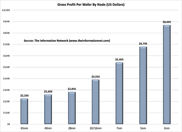
Note: In January 2025, a media report pointed out that for the 5nm and 3nm that TSMC’s US plant intends to produce, before the US subsidy, the production cost per wafer in Taiwan is US$9,566, while the Arizona plant needs US$1,272. , the gap is nearly 30%. After subsidies, the cost drops to US$10,438, with a gap of less than 10%.
Wafer foundry R&D Costs
From the perspective of the cost of advanced process design, according to the calculation of Semi engineering, a third-party semiconductor research institution, the development cost of the 28nm process is about 51.3 million US dollars, and the 16nm process needs to invest 100 million US dollars, and to the 5nm process node, This cost reached $542 million. If calculated according to the nearly double increase, on the 2nm process, the development cost may be nearly 2 billion US dollars. This fee includes IP authorization, software, validation, verification, architecture and other links.
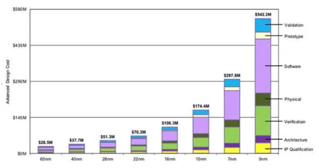
Credit: Semi engineering
The cost of building a chip factory
IBS, a third-party analysis organization, has estimated the R&D investment of wafer fabs in advanced processes. The R&D investment of the 3-nanometer process reaches US$4 billion to US$5 billion. A production line with a 3-nanometer process and a monthly production of 40,000 wafers is built. The cost is about $15 billion – $20 billion.
Therefore, the US$54 billion included in the chip bill passed by the United States this year sounds like a huge astronomical figure. But a chip manufacturing plant with an advanced process needs tens of billions of dollars. You can know that US$54 billion basically does not play a big role in chip manufacturing, which is 20 years behind Asia in the United States, and the symbolic significance is greater than the substantive effect.
Supply chain
Time course required for R&D
The technology of the wafer manufacturing process from R&D to the laboratory is usually a very long and resource-consuming process (including manpower, capital, equipment, software, and materials), which often takes 7 to 10 years. . Take the technical route of the 2nm process as an example; in the semiconductor industry, it was already clear in 2016, and around 2014, research papers have been published.
Until this year, the three major semiconductor manufacturers TSMC, Samsung, and Intel can initially estimate the launch schedule of trial production, which shows how much resources are needed to continue to invest. This is the cruelty of Moore’s Law. Once you can’t keep up with the technological node of a certain chip manufacturing process, you are likely to be left behind forever. It will take far more effort to catch up in the future than everyone can imagine.
The role suppliers play
There are three types of manufacturers that are the most critical in the chip supply chain; including equipment, software (mainly IP and EDA), and materials.
As the advanced process goes down, the number of masks and the complexity of the process will increase significantly, and it will be more difficult to improve the yield. This will not only test design companies, test foundries, but also test equipment manufacturers. Based on the consideration of yield, IP and corresponding complete process design ecology, manufacturers are very cautious when choosing process architecture, and will not replace it unless necessary.
The brand-new process architecture is behind the huge engineering. It involves the replacement of equipment, and the replacement of machines involves cost, yield, and the establishment of a new process architecture ecosystem. TSMC is developing a new process architecture, and the replacement ratio of the machine should not exceed 10% as much as possible, which can ensure the production yield. Another huge project is that IP needs to be rebuilt and re-verified, which undoubtedly has many uncertainties for foundries and design companies to rebuild a new process ecology.
Critical suppliers
Lithography
Please refer to another blog article I wrote before, “ASML, who dominate TSMC’s fate“
EDA
The mainstream tools of the major EDA manufacturer Synopsys (ticker: SNPS) are updated with a fixed cycle of 9 months. There are two types of updates and iterations of EDA tools. One is evolution, which is the most important development method. It mainly enhances the functions of existing tools according to new features and requirements such as processes and applications. This iteration is ongoing.
The development of another EDA tool is revolutionary, leading innovation in the direction of the industry by introducing revolutionary tools and methodologies.
A few years ago, Synopsys worked with the foundry to develop EDA tools for the 2nm process. Before the foundry takes on new customers, they will continue to verify with Synopsys’ EDA tools until they finally pass. A lot of research is parallel, not to say that after the development of 3 nanometers, the development of 2 nanometers began.
The cost of advanced process wafers has skyrocketed. The design cost of 7nm wafers is US$349 million, while the design cost of 5nm wafers will increase to US$476 million. Companies are designing and developing advanced process wafers, result in the cost raising to purchase EDA tools and pay for authorization.
Pricing example: Apple mobile phone SoC
In January 2025, Creative Strategies CEO and chief analyst Ben Bajarin wrote that Apple’s A-series chips continue to evolve, with the A7 processor (used in the iPhone 5S) using a 28nm process and 1 billion transistors. Today’s A18 Pro processor (used in the iPhone 16 Pro) uses a 3nm process, and the number of transistors has jumped to 20 billion.
The 10nm A11 processor and the 7nm A12 processor have seen the largest increases in transistor density, 86% and 69% respectively. However, the recent A16~A18 Pro processors have seen a slower growth in transistor density. This indicates that the current process may be approaching its physical limit.
As the number of transistors increased significantly, the cost also soared, with the price of wafers rising from US$5,000 for the A7 to US$18,000 for the A17 and A18 Pro. The cost per square millimeter of the processor increased from $0.07 to $0.25.
The article states that Apple’s smartphone A-series processors have made significant progress from the A7 to the current A18; and TSMC’s wafer foundry price has also increased 2.6 times from US$5,000 in the A7 era to US$18,000.
It is rumored that Apple is not priced per wafer, but is the “only” customer of TSMC that is priced based on the number of chips; this is a great courtesy for Apple, TSMC’s largest customer.
Intel’s 18A Priced 25% Lower Than TSMC
According to a report by Wccftech, Apple’s adoption of Intel’s 18A process technology is highly attractive. The price of Intel’s 18A process wafers is reportedly about 25% lower than TSMC’s 2nm process, effectively reducing Apple’s future chip production costs. With global memory prices continuing to rise and overall electronic component costs increasing, a lower-cost foundry solution would help Apple maintain product profits and market competitiveness.
SMIC’s 28nm cut price by 40%
In January 2025, SMIC lowered the price of 28nm chips without warning, from US$2,500 per wafer to US$1,500, a 40% drop. The price difference of up to one thousand US dollars was quite rare and shocked the market.
I emphasized in my post “”6 common wrong semiconductor investment myths” that the vast majority of the world’s chips do not require advanced processes. Especially since SMIC will be the world’s third largest wafer foundry by 2024, this price cut will have an important impact on the mature processes of the world, including UMC, World Advanced, GlobalFoundries, and even Samsung and TSMC. If Samsung and TSMC do not force customers to bundle advance and mature processes, prospects will be affected.
TrendForce said that data showed that in 2024, Taiwan’s market share in mature processes will be 44%, leading the world, but China will be close behind with 31%. By 2027, China will make significant progress and increase its market share to 39%. Taiwan’s rate will drop to around 40%, with almost no gap between the two sides. In the future, China will dominate and control the world’s mature process market.
This is why the United States and the European Union have been clamoring to start sanctioning China’s semiconductor equipment needed for mature processes since 2024 because they cannot compete with China’s mature processes. Again!
Conclusion
The 2nm process has just started, and the discussion on the 1.5nm process has already started at the semiconductor technical seminar. After 2025, there will be a new architecture, which the industry calls FortSheet. By 2030, there will be a new The structure is discussed and may become a reality. Moore’s Law will slow, but it will likely continue.
Related articles
- “SK Hynix dominates memory by AI“
- “TSMC has notorious tracking record of violating Labor Law“
- “TSMC CEO appalling remarks on Chinese robots, inferiority to nVidia Huang“
- “SkyWater, 3D chip leader and the only pure-play US chip foundry“
- “Morris Chang refuted by Yeh Wanan, Taiwan was unwilling to invest in TSMC“
- “What does book “Chip War” talk about?“
- “How important is semiconductor industry to Taiwan?“
- “How was TSMC originally founded? Not by Morris Chang“
- “TSMC risks and disadvantages in Taiwan“
- “165 billions investment proved TSMC moat and competitiveness is fragile“
- “Why was ASML founded?“
- “TSMC Morris Chang’s controversial words and deeds“
- “TSMC Advanced Packaging Evolution History“
- “TSMC is becoming the lord of semiconductor packaging, in addition to foundry“
- “Taiwan’s abandoned nuclear hit TSMC hard, profit margins decrease 1% by electricity price increase“
- “What are silicon photonics? Why it’s important? and current progress“
- “Rapidus will be TSMC’s strongest rival in the future“
- “How does Onto make money? Advanced packaging beneficiary“
- “Mong-Song Liang, the hero of SMIC’s breakthrough in US blockade“
- “Why is TSMC valuation much lower than US peers?“
- “TSMC negative toxic corp culture and management style are detrimental to its future and growth“
- “Four chip companies account for one-third of S&P 500 gains so far this year
- “Top five lucrative artificial lucrative intelligence listed companies“
- “What’s TSMC DCF intrinsic value?How to calculate it quickly with a free tool?“
- “How many fabs and houses does TSMC have currently and in the future?“
- “Yield rate comparison of SMIC, Rapidus, TSMC, Samsung, Intel’s advanced process“
- “The TSMC cost, sell price, and R&D cost of chip foundry“
- “ASML, who dominate TSMC’s fate“
- “Comparison of SMIC, Rapidus, TSMC, Intel, and Samsung’s new process roadmaps for future chips“
- “Two long-term threats to TSMC: US and SMIC“
- “Why is TSMC’s profit margin much greater than competitors?“
- “How does TSMC make money?“
- “Zyvex and sub-nanometer semiconductor processes, will Zyvex threat TSMC?“
- “TSMC gets emerging and serious challenges“
- “How does nVidia make money, Nvidia is changing the gaming rules“
- “The reasons for Nvidia’s monopoly and the challenges it faces“
- “Why nVidia failed to acquire ARM?“
- “Revisiting Nvidia: The Absolute Leader in Artificial Intelligence, Data Center, and Graphics“
- “How does Intel make money? and the benefits to invest in it“
- “Intel’s current difficult dilemma“
- “How does Texas Instruments make money? Amazing long term capital reward and company net profit margin!“
- “How AMD makes money? A rare case of turning defeat into victory“
- “Why is AMD’s performance so jaw-dropping?“
- “Qualcomm diversifies success, no nonger highly dependend on phone“
- “How does the ubiquitous Arm make money?“
- “Significant changes in Broadcom’s business approach“
- “Data center, a rapidly growing semiconductor field“
- “How does Applied Materials, lord of semiconductor equipment, make money?“
- “How does Lam Research, top chip equipment player, make money?“
- “The lucrative semiconductor supply chain“
- “Global semiconductor chip market in detail, big dominators and markets“
- “6 common wrong semiconductor investment myths“
- “Gen 3 semiconductor“
- “Three EDA oligopoly vendors: Synopsys, Cadence, and Siemens’s Mentor Graphics“
- “How does, the EDA oligopoly, Cadence make money?“
- “How does Synopsis, the EDA oligopoly, make money?“
Disclaimer
- The content of this site is the author’s personal opinions and is for reference only. I am not responsible for the correctness, opinions, and immediacy of the content and information of the article. Readers must make their own judgments.
- I shall not be liable for any damages or other legal liabilities for the direct or indirect losses caused by the readers’ direct or indirect reliance on and reference to the information on this site, or all the responsibilities arising therefrom, as a result of any investment behavior.
Thanks for this info, Andy.
Hi Chris,
You are welcome and thanks for your visiting. It’s glad to hear my post is helpful and welcome to leave your comments.