I suggest you also read the companion article to this one: “Why was ASML founded?“
TSMC discussion in my books
I have discussed the company Nvidia (ticker:NVDA) in two recent books; including:
In my book “The Rules of Super Growth Stocks Investing“:
- Sections 2-4, the entire section is dedicated to introducing the company TSMC
- Section 3-3, analyze the business development of technology companies to grasp the pulse of key industries
In my book “The Rules of 10 Baggers“:
- Section 3-2, the entire section is dedicated to introducing TSMC and the global semiconductor supply chain.
An ASML (ticker: ASML) lithography machine asking for 100 million euros (about 120 million US dollars, , this is the current model’s rice and will vary with features and models), but you may not get it even you have money.
Please pay special attention: lithography machine and etching machine are two completely different devices. ASML is a lithography machines vendor, not etching machine.
ASML’s stock price and valuation
It is currently the world’s largest semiconductor equipment manufacturer, and the company has only one product. The stock price and valuation are as follows:
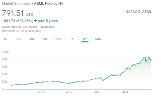
- In the past five years, its stock price has risen by nearly 700%, and in the past ten years, its stock price has risen by nearly 1,115%; as shown in the figure below, it comes from Google Finance.
- Its current market value is US$320 billion
- Price to revenue ratio 16.65
- Price Earnings Ratio 53
The role of lithography
How important is lithography? Lithography is just a general term, which includes many links, and lithography machine (also known as exposure equipment) is the most important equipment. The other is photoresist, an important semiconductor chemical material, and photoresist materials account for about 5% of the total cost.
Dozens of times of photolithography may be required in the entire wafer manufacturing process. The cost of the photolithography process accounts for 35% of the entire wafer manufacturing process, and the time consumption accounts for about 40%-50% of the entire chip production process. Depending on the advanced process and craftsmanship will vary.
Upright monopoly
How important ASML is?
How important is lithography? Lithography is just a general term, which includes many links, and lithography machine (also known as exposure equipment) is the heaviest hardware device. The other is photoresist, an important semiconductor chemical material, and photoresist materials account for about 5% of the total cost.
The reason is that exposure equipment accounts for about 22% of all advanced process manufacturing equipment costs and about 20% of the manufacturing time. In addition, only ASML produces advanced extreme ultraviolet exposure (EUV) equipment. EUV is the essential key to enter the advanced process below 10nm.
Previously, ASML has launched three generations of EUV equipment, namely TWINSCAN NXE: 3400B, NXE: 3400C, and NXE: 3600D, all with a numerical aperture of 0.33. Theoretically, the accuracy of the wafers produced by the third-generation EUV exposure equipment is about 2 nanometers at most. Once the node is below the 2 nanometer, that is, when the micrometer (1 micrometer = 0.1 nanometer), ASML must develop higher precision equipment again. The most advanced exposure equipment is called High NA (High Numerical Aperture) EUV exposure equipment. ASML’s chief technical officer stated in September 2022 that the first High-NA EUV exposure machine will be delivered in 2023, which is the next-generation high-precision EUV exposure equipment model NXE: 5000, 0.55 high numerical aperture EUV Exposure equipment, each selling for up to $400 million.
Any way to bypass ASML?
Although DUV (Deep Ultraviolet Light Exposure) machines are mainly used for chips in mature processes, TSMC and Samsung Electronics can also produce chips with processes below 10nm. For example, TSMC is producing the first-generation 7-nanometer process (N7 node), which is produced through DUV’s 193nm immersion ArF lithography. Benjian Lin, the father of immersion lithography, believes that even without high-end and expensive EVU, it should be no problem for SMIC to achieve at least 5nm with existing equipment, breaking the stereotype that the outside world only stays at 28nm.
Like TSMC, SMIC has used this method and has already successfully shipped 7nm process chips to customers in 2019. The last paragraph of this article will detail the development of the matter.
However, although the line spacing can be reduced after multiple exposure through liquid infiltration using a DUV exposure machine, it has the following major disadvantages:
- It is very difficult to achieve the equivalent of EUV’s 13.5nm wave, that is, to achieve the yield and cost of TSMC’s 7nm process. Because TSMC’s high yield rate in advanced systems is known to everyone in the industry; it’s only a bit worse than its mature manufacturing process, but not much. Samsung’s new advanced manufacturing process is relatively normal, that is, the gap between the yield rate and the yield rate of the mature process is too large. This is one of the main reasons why TSMC has higher gross profit, more customers, and higher market share.
- The entire process of multiple exposure is just too complicated, lengthy, and time-consuming, the probability of error is higher ─ ─ resulting in low yield.
- Multiple exposures will inevitably increase the consumption and waste of power and resources, and will drastically lower net profit eventually.
This is why SMIC has emphasized many times that SMIC has in fact already possessed the capability of more advanced processes from 12nm to 7nm, and it is completely feasible through internal empirical engineering, but it is still willing to wait for ASML’s extreme ultraviolet light exposure ( EUV). The main reason is because it does not meet the cost and economic benefits.
A company really pinch TSMC’s neck
In May 2024, Bloomberg reported: “ASML can remotely shut down ASML’s machines at TSMC.”
Why would I say that?
- It is also true that TSMC (ticker: TSM) also has many key suppliers. But most of them are oligopolistic, or alternative solutions can still be found, or they rely on TSMC more than TSMC ask for them.
- Without ASML’s extreme ultraviolet (EUV) lithography machine, TSMC’s all higher-end processes below 7nm (which is also the source of most of its revenue) would have to be shut down immediately, not only without other suppliers, and there is no alternative at all.
- Look at the SMIC in mainland China. It has money, people, a market, and customers; the only thing it lacks is ASML’s extreme ultraviolet (EUV) lithography machine. If ASML announces that it immediately agrees to ship its extreme ultraviolet lithography machine to SMIC, we can be said with confidence that Taiwan’s share price will immediately fall sharply, and it will continue to bottom out. On the contrary, ASML’s own stock price and SMIC’s stock price will immediately rise sharply and continue to hit new highs. For this part, I suggest you refer to my other blog post “Two long-term threats to TSMC“.
In 2022, Bloomberg Businessweek once made a special report, TSMC accounted for 6% of Taiwan’s electricity consumption in 2020, and it is estimated that it will reach 12.5% in 2025. ASML’s most advanced EUV lithography equipment consumes an estimated power of about 1 million watts (depending on the model), which is more than 10 times the power consumption of previous generations of equipment, but it is the only choice for TSMC for the most advanced process. Bloomberg Businessweek estimated TSMC has more than 80 EUVs.
Competitors
In 2020, the total global sales of lithography machines were 413 units. Among them, ASML sold 258 units accounting for 62%, Canon (ticker: CAJ) sold 122 units accounted for 30%, and Nikon (ticker: NINOY) sold 33 units accounted for 8%. However, the current product level of Nikon and Canon is only about the level of ASML’s next-level deep ultraviolet light source (DUV) level (ASML’s DUV light source lithography machine can still be sold to China, because it is not regulated by the United States). Calculated by sales, because only ASML has the ability to manufacture the most expensive extreme ultraviolet lithography machine, the total market share is 91%, 3%, and 6% in order. So at present, neither Nikon nor Canon can pose a threat to ASML.
Products
Truly exclusive monopoly
I mentioned in the book “The Rules of Super Growth Stocks Investing” that there are very few real monopoly companies in the market, mainly because the government will definitely intervene and it is impossible for this to happen. And as long as it is a monopolistic enterprise, the profit must be substantial, because it must have the power to increase prices, and customers can only be at the mercy of it, as evidenced by ASML’s 120 million US dollar machine. ASML has only a dozen EUV production capacity a year. Therefore, in reality, apart from state-owned enterprises, it is almost impossible for any country to have any independent manufacturers. ASML can be said to be the only company that I can think of at the moment, really super large, in the technology sector, and truly monopoly.
ASML has an absolute advantage in the global semiconductor equipment lithography machines, with a 90% market share in similar products worldwide and a 100% market share below 14 nanometer process.
A new generation of EUV extreme ultraviolet exposure machine
The High-NA EUV exposure machine is ASML’s latest generation of lithography equipment, which will be officially shipped in 2022, which indicates that ASML has taken another big step forward on the road of 0.55 numerical aperture lithography technology. This equipment is a key lithography equipment for future investment in gate-all-around (GAA) technology and 2nm node process. The main foundry manufacturers should be Intel, TSMC, and Samsung. It is reported that they are already conducting installation tests.
At present, the three generations of EUV extreme ultraviolet exposure machines launched by ASML are TWINSCAN NXE: 3400B, NXE: 3400C, NXE: 3600D, and the numerical apertures are all 0.33. In theory, the accuracy of the wafers produced by the third-generation EUV extreme ultraviolet exposure machine equipment can only reach about 2 nanometers at most. It is necessary to develop higher-precision exposure equipment, called High NA (High Numerical Aperture) EUV extreme ultraviolet exposure equipment. The latest next-generation high-precision EUV extreme ultraviolet exposure machine model is EXE: 5000, with a numerical aperture of 0.55, which can be used for wafer fabrication below the 2nm node, such as 1.4nm (14 angstroms), 1 nanometer (10 angstroms) and other processes.
The price of the previous ASML EUV extreme ultraviolet exposure machine is 120 million US dollars, but the price of this latest EUV extreme ultraviolet exposure machine is about 400 million US dollars.
By the way, it is worth mentioning that the Belgian Microelectronics Research Center (IMEC) is the main key technology partner of ASML EUV extreme ultraviolet exposure machine equipment, and IMEC is the key technology provider for many of ASML’s lithography exposures.
Western uses ASML to block Chinese semiconductors
SMIC’s 7nm process already production
As mentioned earlier in this article, the fabrication of 7nm wafers does not require Esmol’s EUV machines at all, and TSMC’s 7nm does not actually use EUV lithography machines. SMIC’s cryptocurrency mining customer MinerVa has long said that SMIC’s 7-nanometer wafers will start production as early as July 2021.
ASML’s policy towards China
SMIC announced in March 2021 that ASML has signed an order for deep ultraviolet (DUV) lithography equipment of US$1.2 billion, with a deadline of the end of 2021.
ASML has repeatedly stated that it maintains an open attitude towards land-based exposure machines and fully supports them within the legal framework. Except for EUV machines, other products can be shipped to land-based customers. In recent years, ASML’s shipments to the continental market accounted for 30% of the global sales, and the previous installed capacity in the mainland was close to 1,000 units.
However, it has been reported recently that in order to completely block the semiconductor industry in mainland China, the United States has planned to extend the ban to a mature manufacturing process starting in 2022. In other words, once the new ban comes true (this new ban has too much impact and may hurt many American manufacturers), ASML will not even be able to export DUV lithography equipment to mainland China.
The West’s move to block China seems to fall short
Beijing authorities have identified the semiconductor supply chain and dealt with it as a “national emergency.”
In June 2021, ASML’s chief executive publicly stated that the implementation of an embargo on China’s cutting-edge lithography machines will result in China’s own R&D and manufacturing, which may result in technological breakthroughs in three years. The machine market was shocked and even forced ASML to withdraw from the market. Judging from past experience, as long as China masters this technology, China’s production costs will be cheaper than internationally. At that time, ASML may have withdrawn from the world lithography machine market. What I want to say is that competitors’ comments on the company are not only the most valuable for reference, but also the most accurate (Buffett once had a similar view).
Previously, SMEE (Shanghai Microelectronics), a domestically produced lithography machine in China, has already claimed to enter 28nm and 14nm since mid-2020, but the yield rate of finished products was not high at that time. However, on 11/26/2021, the mainland Chinese media IT House reported that Foxconn’s first packaging and testing plant in Qingdao, Shandong Province, introduced 46 sets of 28-nanometer lithography machines made by Shanghai Microelectronics made in China in one go. This is an amazing achievement. The domestic lithography machine that represents mainland China has broken through from 90nm to 28nm in just a few years. It’s just that everyone should pay special attention that these lithography machines currently delivered can only be used for the packaging of advanced wafers and cannot be used for production.
Closing words
As the title of this article says: ASML, who dominate TSMC’s fate.

Related articles
- “SK Hynix dominates memory by AI“
- “Teradyne, semiconductor back-end automated test equipment leader“
- “TSMC has notorious tracking record of violating Labor Law“
- “How KLAC makes money, the largest equipment supplier for chip quality control“
- “TSMC CEO appalling remarks on Chinese robots, inferiority to nVidia Huang“
- “SkyWater, 3D chip leader and the only pure-play US chip foundry“
- “Morris Chang refuted by Yeh Wanan, Taiwan was unwilling to invest in TSMC“
- “What does book “Chip War” talk about?“
- “How important is semiconductor industry to Taiwan?“
- “Why was ASML founded?“
- “ASML, who dominate TSMC’s fate“
- “TSMC risks and disadvantages in Taiwan“
- “165 billions investment proved TSMC moat and competitiveness is fragile“
- “Camtek: A little-known but outstanding semiconductor equipment supplier”
- “How was TSMC originally founded? Not by Morris Chang“
- “TSMC Morris Chang’s controversial words and deeds“
- “TSMC is becoming the lord of semiconductor packaging, in addition to foundry“
- “What are silicon photonics? Why it’s important? and current progress“
- “Rapidus will be TSMC’s strongest rival in the future“
- “How does Onto make money? Advanced packaging beneficiary“
- “Top five semiconductor equipment providers“
- “Mong-Song Liang, the hero of SMIC’s breakthrough in US blockade“
- “TSMC negative toxic corp culture and management style are detrimental to its future and growth“
- “Four chip companies account for one-third of S&P 500 gains so far this year
- “Top five lucrative artificial lucrative intelligence listed companies“
- “Why is TSMC valuation much lower than US peers?“
- “What’s TSMC DCF intrinsic value?How to calculate it quickly with a free tool?“
- “How many fabs and houses does TSMC have currently and in the future?“
- “Yield rate comparison of SMIC, Rapidus, TSMC, Samsung, Intel’s advanced process“
- “The TSMC cost, sell price, and R&D cost of chip foundry“
- “Comparison of SMIC, Rapidus, TSMC, Intel, and Samsung’s new process roadmaps for future chips“
- “Two long-term threats to TSMC: US and SMIC“
- “Why is TSMC’s profit margin much greater than competitors?“
- “How does TSMC make money?“
- “Zyvex and sub-nanometer semiconductor processes, will Zyvex threat TSMC?“
- “TSMC gets emerging and serious challenges“
- “How does nVidia make money, Nvidia is changing the gaming rules“
- “The reasons for Nvidia’s monopoly and the challenges it faces“
- “Why nVidia failed to acquire ARM?“
- “Revisiting Nvidia: The Absolute Leader in Artificial Intelligence, Data Center, and Graphics“
- “How does Intel make money? and the benefits to invest in it“
- “Intel’s current difficult dilemma“
- “How does Texas Instruments make money? Amazing long term capital reward and company net profit margin!“
- “How AMD makes money? A rare case of turning defeat into victory“
- “Why is AMD’s performance so jaw-dropping?“
- “Qualcomm diversifies success, no nonger highly dependend on phone“
- “How does the ubiquitous Arm make money?“
- “Significant changes in Broadcom’s business approach“
- “Data center, a rapidly growing semiconductor field“
- “How does Applied Materials, lord of semiconductor equipment, make money?“
- “How does Lam Research, top chip equipment player, make money?“
- “The lucrative semiconductor supply chain“
- “Global semiconductor chip market in detail, big dominators and markets“
- “6 common wrong semiconductor investment myths“
- “Gen 3 semiconductor“
- “Three EDA oligopoly vendors: Synopsys, Cadence, and Siemens’s Mentor Graphics“
- “How does, the EDA oligopoly, Cadence make money?“
- “How does Synopsis, the EDA oligopoly, make money?“
Disclaimer
- The content of this site is the author’s personal opinions and is for reference only. I am not responsible for the correctness, opinions, and immediacy of the content and information of the article. Readers must make their own judgments.
- I shall not be liable for any damages or other legal liabilities for the direct or indirect losses caused by the readers’ direct or indirect reliance on and reference to the information on this site, or all the responsibilities arising therefrom, as a result of any investment behavior.
The multiple exposure argument doesn’t work to justify EUV since EUV also needs multiple exposures.
Hi Fred,
Glad to have your inputs. I agree with your comment. This is is why theory is just theory, if it’s feasible, SMIC will apply ‘the theory’ on DUV, SMIC should have their 7nm on production last year or earlier, and customers will flock to SMIC for 7nm process.
Although Ben Lin said several times, SMIC should be able to have ‘up to 4nm’ process by existing DUV machines, I doubt it is feasible for mass production, as you explained and what I listed in my post.
TSMC EUV process is already multipatterning, at least half the masks are for cutting pre-patterned lines. SMIC is limited by market currently, it seems even 14nm volume is low or disappeared. That’s a relatively mature process, developed with Qualcomm and imec (and Huawei). If no 14nm demand, can wait on 7nm or less.
Fred,
Thanks for your inputs, your are the expert in the filed and it’s our pleasure to welcome your visiting and insight comments.