Gen 3 semiconductor are a very new field in terms of the entire “The lucrative semiconductor supply chain“.
Introduction
First, Second, and Third gen semiconductor
The generation one semiconductor materials were mainly silicon and germanium. After the 1960s, silicon-based semiconductors gradually became the mainstream and are still the most widely used semiconductor materials. More than 95% of the world’s wafers are still based on silicon-based wafers.
The gen 2 semiconductor material is mainly gallium arsenide (GaAs) and indium phosphide (InP). The representative is gallium arsenide, which can manufacture higher frequency and high-speed integrated circuits. However, the bandwidth of the material is still small.
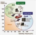
The third generation of semiconductor materials is born in response to the times. Materials represented by silicon carbide (SiC) and gallium nitride (GaN) can prepare high-voltage and high-frequency power devices. Among them, silicon carbide has the best comprehensive performance and is commercialized. The third-generation semiconductor material with the highest degree and the most mature technology.
A breakthrough in semiconductor
Many people think that third-generation semiconductors, like advanced manufacturing processes, are accumulated from the technologies of first- and second-generation semiconductors, but this is not the case. These three generations of semiconductors are actually in a parallel state, developing their own technologies; there is no technical interdependence between them.
That is, silicon carbide is not a gradual improvement of the original technology, but a leap upgrade. This is why mainland China has written the development of third-generation semiconductors into the country’s roadmap for future technological development in an environment where traditional silicon-based semiconductors are monopolized and deliberately obstructed by the West. The third gen semiconductor, the term that we commonly use now, are actually terms invented in China.
In the face of the continuous suppression of the United States in the semiconductor field, the mainland China wants to use the third-generation semiconductor technology to surpass the United States. Bloomberg reported that the mainland not only decided to invest 10 trillion yuan in the research and development and production of third-generation semiconductor materials. It was written into the national plan of the “Tenth Five-Year Plan” of China for the first time.
What’s the advantages?
The third-generation semiconductor materials are especially suitable for high-frequency, high-voltage, and high-temperature operating environments to exhibit excellent power conversion efficiency, which can save power and reduce energy consumption. The two main application areas are radio frequency and power conversion.
Application areas
The main application scenarios of third-generation semiconductors include: new energy vehicle power devices, solar inverters (PV inverter or solar inverter), 5G equipment RF devices, charging piles, traction inverters, etc.
The proportion of the amount occupied by various application scenarios is taken as the average of 2020 and 2021, namely: new energy vehicles 49.93%, solar energy 10.92%, 5G base stations 27.68%, charging piles 4.44%, and inverters 7.03%.
The market size
TSMC’s view
To use the words of Mark Liu, chairman of TSMC (ticker: TSM), compared with the existing semiconductor industry market dominated by silicon, the third-generation semiconductor is actually a very small market. At present, TSMC only provides foundry services such as 6-inch GaN on Si (gallium nitride on silicon), GaN on SiC (gallium nitride on silicon carbide) and other foundry services, but compared with traditional silicon wafer foundry, the amount is very small, it can be ignored directly, which is why Mark Liu has such a comment.
Research institites estimation
Yole data shows that silicon is still the mainstream of semiconductor materials, accounting for 95%. As the penetration rate of the third-generation semiconductor increases year by year, in 2023, the penetration rate of silicon carbide is expected to reach 3.75%, and the penetration rate of gallium nitride will reach 1.0%, and the combined penetration rate of the third-generation semiconductor can reach 4.75%.
According to TrendForce’s estimates, from 2020 to 2025, the market of gallium nitride will grow from $48 million to $850 million, and silicon carbide will grow from $680 million to $3.39 billion, with a compound annual growth rate. The rates were 78% and 38%, respectively. According to the forecast of Yole Developpement, a French market research institute, the market size of silicon carbide power chips in 2026 will be 6 times higher than that in 2020, reaching US$4.48 billion.
If compared with the overall semiconductor market, in 2020, the output value of gallium nitride plus silicon carbide will only account for three thousandths of all semiconductors, or about 0.3%; by 2025, it will grow to six thousandths , and only 0.6%. Compared with the current first- and second-generation semiconductor markets, it can be said that it is only a very small market.
Impossible to replace silicon-based semiconductor
No matter which market research company estimates, there is only one conclusion. Even if third-generation semiconductors have unparalleled and proven uses and benefits in power conversion, please don’t deify third-generation semiconductors. The third generation of semiconductors and the first and second generations are not substitutes, but complementary. The era of silicon will not end, but after the third-generation semiconductor gradually increases the penetration rate, it will definitely squeeze the penetration rate of silicon.
At least for the foreseeable five years, it is still a very small market in the semiconductor market, and it is certain that it is impossible to replace the existing silicon-based semiconductor world in the foreseeable future.
Two wafer materials
The gen 3 semiconductor materials are silicon carbide (SiC) and gallium nitride (GaN).
Gallium nitride
Please see the in-depth discussion in the article “Gen 3 Semiconductor Gallium Nitride” that I will post here in a while.
Silicon carbide
Compared with gallium nitride, silicon carbide is mainly used in large-scale applications such as electric vehicles and wireless communications. This part deserves an in-depth discussion, which I will explore in two future articles. See “The hot silicon carbide” and “Wolfspeed, the upstart of the third-generation semiconductor silicon carbide”
Leading vendors’ latest performance
The Philadelphia Semiconductor Index (SOX) has fallen by 26.53% in the past six months (as of September 21). But at this time, the third-generation semiconductor materials represented by silicon carbide and gallium nitride are ushering in market doubling and capacity expansion.
ON Semiconductor
After the release of the second quarter financial report of ON Semiconductor (ticker: ON), it raised its 2022 silicon carbide revenue forecast to a “three times year-on-year growth”, while the previous target was only a 1-fold increase; it is expected that by 2023, the silicon carbide business will increase Revenue will exceed $1 billion. 3x is just the beginning, not even 10x: ON Semiconductor also plans to expand the company’s SiC front-end process capacity to more than 10x its current capacity by 2025.
STMicroelectronics
STMicroelectronics (ticker: STM) second-quarter financial report also expects that ST’s silicon carbide business will receive $700 million in revenue in 2022 and $1 billion in 2023. STMicroelectronics is also a major supplier of Tesla’s silicon carbide power modules. Mainly benefiting from the demand for silicon carbide in the automotive, industrial and other fields, STMicroelectronics is also planning to expand production.
Wolfspeed
Wolfspeed (ticker: WOLF) also announced in the first half of this year that it will build a new silicon carbide plant in Chatham County, North Carolina, which will become the world’s largest silicon carbide material plant when completed in 2030. Its silicon carbide wafer manufacturing capacity It has increased by about 13 times, and currently the silicon carbide produced by Wolfspeed has accounted for more than 60% of the global silicon carbide. The total investment in the new factory will reach $5 billion, for which Wolfspeed will also apply for federal grants related to the “Chip Act”.
For this company deep dive, please refer to my post “Wolfspeed, the upstar of gen 3 semiconductor“.
Related articles
- “What are silicon photonics? Why it’s important? and current progress“
- “The lucrative semiconductor supply chain“
- “How does ON Semiconductor make money? Experts in power and analog signal processing and sensor“
- “Gen 3 semiconductor“
- “The hot gen 3 silicon carbide (SiC)“
- “Wolfspeed, the upstar of gen 3 semiconductor“
- “TSMC negative toxic corp culture and management style are detrimental to its future and growth“
- “Four chip companies account for one-third of S&P 500 gains so far this year
- “Top five lucrative artificial lucrative intelligence listed companies“
- “Why is TSMC valuation much lower than US peers?“
- “What’s TSMC DCF intrinsic value?How to calculate it quickly with a free tool?“
- “How many fabs and houses does TSMC have currently and in the future?“
- “Yield rate comparison of SMIC, Rapidus, TSMC, Samsung, Intel’s advanced process“
- “The TSMC cost, sell price, and R&D cost of chip foundry“
- “ASML, who dominate TSMC’s fate“
- “Comparison of SMIC, Rapidus, TSMC, Intel, and Samsung’s new process roadmaps for future chips“
- “Two long-term threats to TSMC: US and SMIC“
- “Why is TSMC’s profit margin much greater than competitors?“
- “How does TSMC make money?“
- “Zyvex and sub-nanometer semiconductor processes, will Zyvex threat TSMC?“
- “TSMC gets emerging and serious challenges“
- “How does nVidia make money, Nvidia is changing the gaming rules“
- “The reasons for Nvidia’s monopoly and the challenges it faces“
- “Why nVidia failed to acquire ARM?“
- “Revisiting Nvidia: The Absolute Leader in Artificial Intelligence, Data Center, and Graphics“
- “How does Intel make money? and the benefits to invest in it“
- “Intel’s current difficult dilemma“
- “How does Texas Instruments make money? Amazing long term capital reward and company net profit margin!“
- “How AMD makes money? A rare case of turning defeat into victory“
- “Why is AMD’s performance so jaw-dropping?“
- “Qualcomm diversifies success, no nonger highly dependend on phone“
- “How does the ubiquitous Arm make money?“
- “Significant changes in Broadcom’s business approach“
- “Data center, a rapidly growing semiconductor field“
- “How does Applied Materials, lord of semiconductor equipment, make money?“
- “How does Lam Research, top chip equipment player, make money?“
- “The lucrative semiconductor supply chain“
- “Global semiconductor chip market in detail, big dominators and markets“
- “6 common wrong semiconductor investment myths“
- “Gen 3 semiconductor“
- “Three EDA oligopoly vendors: Synopsys, Cadence, and Mentor Graphics“
- “How does, the EDA oligopoly, Cadence make money?“
- “How does Synopsis, the EDA oligopoly, make money?“
Disclaimer
- The content of this site is the author’s personal opinions and is for reference only. I am not responsible for the correctness, opinions, and immediacy of the content and information of the article. Readers must make their own judgments.
- I shall not be liable for any damages or other legal liabilities for the direct or indirect losses caused by the readers’ direct or indirect reliance on and reference to the information on this site, or all the responsibilities arising therefrom, as a result of any investment behavior.